FE gate stack with a tunnel dielectric insert results in larger memory window for NAND applications
It has been nearly 10 years since NAND memory devices went vertical and rapidly evolved into stacks consisting of 230+ layers and with logical scaling up to 3 bits or 4 bits per cell. Today, 3D NAND devices, with their superior bit areal density, cost, and performance, have essentially replaced 2D NAND. But as NAND continues evolving towards 1000+ layer vertical NAND, it faces multiple new technological challenges. One such challenge is that the lateral charge migration in a NAND cell utilizing a conventional charge trap layer, e.g., SiN, is becoming more problematic as device dimensions are scaled down to enable higher-density memory. As a result, issues such as cell-to-cell interference and poor data retention are raising reliability concerns.
To address these challenges, SRC/DAPRA JUMP 2.0 Georgia Tech researchers, working with JUMP 2.0 sponsors such as Samsung, have shown that the introduction of a ferroelectric (FE) as a replacement for the charge trap layer improves the retention of programmed states due to its polarization-bound charge.
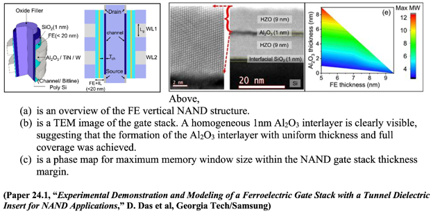
In addition, for a ferroelectric to be considered as a replacement for a conventional charge trap layer, it needs to meet some basic design constraints such as having a thickness less than 19nm, a write voltage less than 15 V, and a memory window (MW) greater than 6.5 V. At IEDM 2023, Georgia Tech researchers modeled and experimentally demonstrated for the first time an Al2O3 layer in the middle of a FE Hafnium Zirconium Oxide (HZO) stack. It significantly enhanced the device’s memory window, from 3V in a reference HZO gate stack without the Al2O3 insert, to as high as 7.3 V, a >2x improvement. The researchers say modeling suggests a pathway to achieving a 12V memory window for vertical NAND flash technology.
This exciting work on an FE replacement for the charge trap layer in NAND is just one of several projects in the JUMP 2.0 PRISM Center looking to improve various aspects of potential future NAND devices. It is a collaboration between SUPREME Scholar Dipjyoti Das and Principal Investigator (PI) Asif Khan, PRISM PIs Shimeng Yu and Suman Datta, and Samsung engineers.