Transforming Today’s Challenges into Tomorrow’s Innovations

In recent decades, the proportion of global semiconductor manufacturing based in the United States has sharply declined. Today, the United States possesses only 12% of the world’s chip manufacturing capacity, compared to 37% in 1990. A significant portion of the world’s GDP is now generated using equipment dependent on semiconductors, and it is both an economic and strategic imperative for the U.S. to strengthen its position in microelectronics manufacturing. Indeed, the United States does not produce the most advanced logic and memory chips, the kind that drive PCs and smartphones, at any commercial scale. In direct response, the U.S. government enacted the CHIPS and Science Act, providing massive new funding and creating a steady stream of support and resources for future advancements.
While having financial resources is important, it's equally crucial to have a clear vision to effectively steer investments towards meaningful outcomes. We must invest wisely to create an enduring, sustainable semiconductor ecosystem. With guidance from the Microelectronics and Advanced Packaging Technologies (MAPT) Roadmap, Semiconductor Research Corporation (SRC) is poised to lead the industry into the next phase of transformative change. Working together, we can immediately begin tackling the ambitious goals outlined in the CHIPS Act.
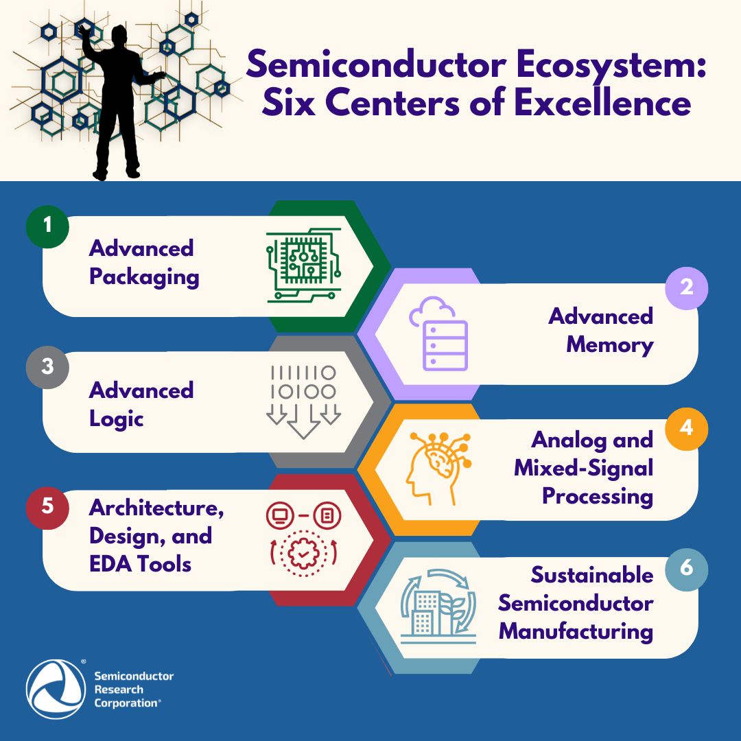
We envision creation of six major capabilities – components of the new semiconductor manufacturing ecosystem shown in the Figure: Advanced Packaging, Advanced Memory, Advanced Logic, Analog and Mixed-Signal Processing, Architecture, Design and EDA, and Sustainable Semiconductor Manufacturing. Below we offer some insights on each of the six capabilities.
Traditional semiconductor technologies that relied on feature-size reduction (dimensional scaling) are reaching their physical limits. Advanced packaging provides an alternative avenue for innovation in density and size of products. In short, advanced packaging is based on the growing use of diverse chiplets positioned inside the same encapsulation. The chiplets can be stacked in three dimensions, known as 3D heterogeneous integration. This allows for compact, cost-efficient, and very capable systems-in-package (SiP), which extends the application space almost to infinity. Advanced packaging with 3D heterogeneous integration opens new avenues for a drastic improvement in energy efficiency of semiconductor chips as it supports tighter integration of processor and memory with photonic interconnects and I/Os. NAPMP’s advanced packaging piloting facility will not only accelerate the transfer of innovations into U.S. manufacturing but also serve as a vital bridge, preventing promising developments from succumbing to the valley of death.
As data generation burgeons exponentially, the demand for high-capacity, high-speed memory solutions surges. Research in advanced memory technologies encompasses a spectrum of approaches, including 3D NAND and 3D DRAM. These efforts aim to overcome the limitations of traditional memory architectures in terms of density, speed, and energy consumption. By pushing the boundaries of memory technology, researchers facilitate the realization of faster energy-efficient computing systems, seamless multitasking, and enhanced storage capabilities essential for modern applications.
The ongoing energy crisis, exacerbated by the widespread integration of AI technologies, emphasizes the need for very low-power chips. We need more than 1000x improvement in computing energy efficiency over the next two decades. This drives research in advanced logic technology. This area encompasses innovations in transistor scaling, novel materials, and alternative computing paradigms such as in-memory computing, neuromorphic computing, etc. Analog and mixed-signal processing play a crucial role in interfacing the digital world with the physical environment. Research efforts focus on developing precision analog circuits, high-speed data converters, and low-power sensor interfaces to enable seamless integration of digital and analog functionalities. Advancements in this domain are instrumental in diverse applications ranging from wireless communication and Internet of Things (IoT) devices to medical electronics and automotive systems, where reliability, accuracy, and energy efficiency are paramount.

Efficient design methodologies and electronic design automation (EDA) tools are indispensable for realizing complex semiconductor systems. Research in this area encompasses architectural exploration, design automation algorithms, and verification techniques aimed at enhancing productivity, reliability, and time-to-market for semiconductor products. By fostering collaboration between academia and industry, researchers drive innovation in system-on-chip (SoC) design, enabling the seamless integration of diverse hardware and software components while addressing the challenges posed by increasing design complexity and heterogeneity.
With growing environmental concerns and resource constraints, sustainable semiconductor manufacturing has emerged as a pressing imperative. R&D endeavors in this realm encompass the commercial certification of eco-friendly materials, energy-efficient fabrication processes, and waste reduction strategies aimed at minimizing the environmental footprint of semiconductor production. By qualifying and adopting green manufacturing practices and recycling initiatives, researchers strive to mitigate pollution, conserve resources, and promote the long-term sustainability of the semiconductor industry.
As government, academics, and industry move together to shape the future of semiconductor technology, SRC offers a plan that will meet the needs outlined in the Decadal Plan for Semiconductors. By fostering innovation across these six crucial domains, researchers pave the way for transformative advancements that shape the future of electronics and beyond. Embracing a collaborative and interdisciplinary approach, the semiconductor research community continues to push the boundaries of what is possible, ushering in an era of unprecedented technological innovation and societal impact. The time to act is now.


