
Technical scope of nanoelectronic COmputing REsearch (nCORE) program
Mission and Objective
The nanoelectronic COmputing REsearch (nCORE) program funds collaborative university research in the U.S. to develop key technologies to enable novel computing and storage paradigms with long-term (10-20 years) impact on the semiconductor, electronics, computing, and defense industries. The nCORE program supports the National Strategic Computing Initiative (NSCI) through government-industry-academia collaborations. It is driven by fundamental research on novel materials and devices with the potential to achieve significantly improved efficiency, enhanced performance, and new functionalities, beyond the capability of conventional CMOS technologies. The funded research will explore and characterize small integrated systems that can be benchmarked, modeled, and robustly manufactured for future semiconductor applications. The new program is built upon the learning from the Nanoelectronics Research Initiative (NRI).
Program Scope
The research scope of the nCORE program is described by five research vectors. This forward focused program will include activities that increase fundamental knowledge and establish technical expertise in these research vectors.
Research Vector 1: Novel computing and storage paradigms, and theory of operation, beyond conventional CMOS devices, beyond von Neumann architectures, or beyond classical information processing and sensing
Research Vector 2: Fundamental material, device, and interconnect research to enable novel computing and storage paradigms
Research Vector 3: Advanced manufacturing and nanofabrication to enable the fabrication of emerging devices and systems
Research Vector 4: Innovative metrology and characterization to support basic device and material research, and test platforms and standards to benchmark performance from devices up to systems
Research Vector 5: Computational models to support basic research from emerging devices and materials to novel systems
The five research vectors describe a vertically integrated research structure of a multi-university nCORE center, as shown in Figure 1. Vector 1 defines the high-level objectives of the research center. It includes a broad range of topics in novel computing and storage paradigms. A proposal should focus on selected topics relevant to the expertise of the center or team. Vector 2 is the core of the new program that provide key enabling technologies to achieve the objectives defined in vector 1. A successful center proposal should be driven by innovations in this vector. Vectors 3, 4, and 5 all provide essential support in proposed research. A proposal should incorporate this vertically integrated research structure and address selected research components in each vector; however, it is not required to emphasize each vector equally. The center focus should be based on the expertise and the objective of the team. A proposal may emphasize a particular research vector that is essential to enable a comprehensive research structure represented by Figure 1.
The transformative and translational research anticipated to be the product of any nCORE center needs to be carefully documented, to include the thought process that guided the design of experiments to achieve the anticipated outcomes, as well as clear documentation of the methodology used in making measurements and analyzing data. Benchmarking activities, which are necessary for making informed decisions along the research path, should strive to assign confidence levels to reported parameters and facilitate model and theory development and validation. Ultimately, the results from different center activities should provide a foundation for defining the potential and limitations of materials, device designs, architectures, and computing paradigms.
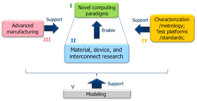
Figure 1. The five research vectors of nCORE representing a vertically integrated research center
Detailed descriptions of technical scope
This section describes in detail the definition of each research vector and suggested research topics.
Research Vector 1
Novel computing and storage paradigms, and theory of operation, beyond conventional CMOS devices, beyond von Neumann architectures, and beyond classical information processing/sensing
The research in the nCORE program aims at enabling computing and storage paradigms to improve efficiency (e.g., low power or energy), to enhance performance (e.g., high computational throughput), and to create novel functionalities (e.g., cognitive capability, information inference). To achieve these goals, the research scope extends beyond CMOS device and design (e.g., low-voltage switch), beyond von Neumann architectures (e.g., compute in memory), beyond classical information processing/sensing, or beyond established algorithms in bio-inspired computing. Different from the JUMP focus on applications and systems, the nCORE program will focus on basic long-horizon material and device research to provide enabling technologies for novel computing and storage paradigms beyond the capabilities of conventional CMOS.
Suggested research topics include, but are not limited to:
- New memory, beyond-CMOS technologies and nano-functions, algorithms, and programming paradigms to address novel computing architectures and the underlying emerging hardware properties and physics (e.g. latency, non-volatility, stochasticity, failure modes).
- Realizing a paradigm shift in how memory is used and accessed through a more optimal hardware platform that takes a holistic, vertically-integrated approach to high-performance “intelligent” storage systems
- Novel architectures with reduced data movement and communication needs, and novel algorithms to optimize data movement strategies adaptively as system loads and usage patterns vary.
- Development of foundational theory for neuromorphic and bio-inspired computing based on novel devices including novel implementation of neurons/neural circuits and programming paradigms. Particular interest lies beyond existing state of the art in deep learning networks, and beyond Deep Neural Network (DNN)/Convolutional Neural Network (CNN) and sparse coded data methods.
- Transduction methods important for new architectures: to preserve salient features of state variables for transmission and subsequent decoding.
- Development of flagship applications for the demonstration and benchmarking of hardware, methods, and computing paradigms.
- Demonstration of novel computing techniques to a scale relevant to real-world problems.
- Prototype concepts in real hardware or emulated hardware in addition to simulation.
- Breakthrough research for autonomous edge of the network distributed computing, utilizing novel methods for energy-efficient communication and data processing
- Development of novel computing and storage paradigms in which the hardware security is intrinsic to the architecture
Research Vector 2
Fundamental material, device, and interconnect research to enable novel computing and storage paradigms
A paradigm shift in information processing and storage is targeted with the goal of enabling novel solutions that profoundly enhance computing and memory capabilities, including support architectures. This will require materials, devices, and interconnects with unique characteristics to provide superior performance, which may also necessitate unconventional and hitherto unknown mechanisms. A comprehensive approach for the system components, sensing, memory/storage, and interconnect is envisioned to build these new energy-efficient, high-performance computation and information processing systems.
Research in novel material systems and interface properties, such as III-V, low dimensional (0D-2D materials), multiferroics, ferroelectrics, magnetics, phase change, metal insulator transitions, will be essential. To support new material systems, new atomically-precise deposition and removal (etch and clean) methodologies are required with suitability for large area, low defect, tight geometries (sub-10 nm) and 3D integration, with selectivity and high-throughput (research vector 3). Paramount to a successful project will be a thorough understanding of heterogeneous system science, including bulk, surface, and interface, and their impact on device physics, without losing sight of the suitable scaling behaviors at sub 10 nm dimensions.
As devices continue to shrink in size, the physics of reduced dimensional systems, including 2D, 1D, and 0D become increasingly important and quantum effects become both beneficial and deleterious. Ultimately, these devices need to be fast, capable of being thermally managed, robustly manufactured, and sufficiently low energy. Understanding the key characteristics required to make them both robust and reliable is crucial to the final design of future devices and essential to the development of next generation characterization tools and metrologies essential to manufacturing. Developing the knowledge infrastructure to characterize and weigh the tradeoffs as one transitions between reduced dimensions is integral to creating functional circuits and architectures. Understanding how to preserve, transduce, and transmit the essential properties of state variable over multiple length scales and across dimensions may also prove critical to future computing. To assess a study’s potential and progress, a plan for development, measurement and tracking of performance parameters and figure-of-merits (FOMs) is mandatory.
Suggested research topics include, but are not limited to:
- Basic research on growth/synthesis methods of new materials with some consideration given to substrate properties and interactions. Explore novel material properties at reduced dimension and new state variables that emerge from dimensional scaling. Research to quantify transitions from uncorrelated many body to correlated few body and beyond (e.g. quantized charge, neutral or ionized excited state, or nuclear state) relative to chemical and physical structure and dimension. Studies to characterize the range (temperature, length, time, electrical bias, etc.) over which a state variable can be maintained.
- Low-power, low-voltage, beyond-CMOS logic and memory devices for von Neumann computing.
- Steep-slope devices with large Ion/Ioff ratios beyond TFET and negative-capacitance FET
- Devices based on phase transition, lattice distortion, interface mechanisms and other transduction mechanisms
- E.g., devices based on metal-insulator transition, charge density wave (CDW), or strain
- Spin-based logic and memory devices
- Sub-ns switching speed with low applied current density
- Orders of magnitude improvement in tunnel magneto-resistance (TMR) in perpendicular magnetic anisotropy (PMA) junctions
-
High spin-polarization through spin-filtering barriers
- 10x improvement in charge-spin conversion efficiency, e.g. research on spin orbit coupling, Rashba interface, and topological insulator materials
- Magneto-electric and magneto-strictive switching mechanisms to enable orders of magnitude improvement in energy efficiency
- Spin-based devices, exploiting novel mechanisms
- Magnetic memories in tiered and embedded applications, e.g., ultra-fast switching enabled by anti-ferromagnetism, giant spin Hall effects for novel device design, etc.
- Beyond CMOS devices, memory elements and materials for non von Neumann computing.
- Novel materials and devices with intrinsic properties suitable for hardware acceleration of machine learning, artificial neural networks, and other bio-inspired information processing
- Devices capable of nanofunctions (e.g., native multiplication, addition, division) with fidelity
- Memory elements and selector devices for novel array computing and storage
- Explore devices leveraging other state variables in addition to charge and spin (e.g., electro-chemical, electro-biological, photonic, phase) to achieve significantly improved performance, information density, or energy efficiency.
- IoT related materials and devices.
- Ultra-low power devices and designs for sensing, information processing, storage, and communication in sensor node/network for IoT
- Materials and devices on unconventional and/or flexible substrates for large area in-sensor computing and machine learning
- Materials and devices for energy generation, scavenging, storage and management for size- and weight-constrained platforms
- Beyond-CMOS devices and materials for THz communication and sensors
- Devices enabling high-density, fine-grained, monolithic 3D systems for reducing data movement and communication cost, e.g. in-sensor/in-memory computing.
- Devices and circuits for security, e.g. Physical Unclonable Functions, random number generators.
- Interconnect.
- Technologies that enable sub-10nm electronic interconnect, including conductors, dielectrics, and their integration methods
- Novel metals and composites as replacement of current metals
- Novel self-alignment and self-assembly techniques to improve integration density
- Self-forming barriers and novel 2D barrier materials
- Reduced dimension interconnects and contacts; low dimensional interconnects with novel transmission properties, e.g. the ability to preserve coherent or correlated states
- Efficient (high speed, low loss) interconnects for a range of state variables, including native interconnect for novel devices that use alternative state variables
- Programmable, high fan-in and fan-out interconnect solutions
- Photonic switching devices and interconnect meeting the E/bit, E/bit/micron, BW/micron requirements competitive against electrical interconnects
- Super-linear, wide-bandwidth electrical and optical links enabling high modulation formats
Research Vector 3
Advanced manufacturing and nanofabrication to enable the fabrication of emerging devices and systems
Novel materials and devices require advanced fabrication technologies, e.g., atomic-scale precision placement, deposition, patterning, and etching. Advanced integration technologies (e.g., monolithic 3D) may enable functional diversification. With number of processing steps approaching thousand and number of critical lithographic layers over fifty, the cost of manufacturing threatens the economic viability of semiconductor industry. As feature sizes approach molecular dimensions, the light source resolution is not the only roadblock anymore. Patterning pitfalls can be mitigated by new patterning material paradigms, precise material placement, planarization and etching techniques (e.g., atomic-scale selective deposition and etching). Other avenues for improvement include all mainstream materials, intelligent functionalizing (Jahn-Teller) or templating materials, and bio inspired manufacturing. Control of processing, interfaces, and defects is also crucial and will require advanced metrology tools capable of nanometer resolution. Stringent form factors for novel cyber-physical systems will require novel packaging techniques. Manufacturing research in new materials, processes, and tools with control at the molecular and atomic levels is critical to provide a cost effective path to the production of reliable future devices and interconnect architectures. Use of novel materials and processes may require novel testing techniques.
Suggested research topics include, but are not limited to:
- New methods to reproducibly fabricate devices and related circuit elements at reduced dimension and physical sizes ranging from micron to nano to meso to atomic length scales.
- Deposition: chemicals, materials and techniques for film deposition with atomic-level precision (e.g., ALD), extreme uniformity and conformality, high selectivity, high throughput, and low thermal budget, including strain mediated processes; deposited films can be dielectrics, semiconductors (1D-3D), conductors, multifunctional materials (e.g., multiferroic, ferroelectric, ferromagnetic), and materials to expand work function selection.
- Self-assembly: novel materials, chemistry, processes for directed self-assembly of nanoscale objects from solution with atomic level precision, including biological templating, chemical recognition, and co-polymer systems.
- Patterning: novel photolithographic materials enabling reduced sidewall roughness, minimum exposure dose, and nm-level resolution.
- Interfaces: novel surface cleaning, surface reconstruction and passivation; material functionality defined by interfaces; control of trap states; understanding of surface interactions of passivating agents and substrates on the atomic scale with ab initio computer simulation.
- Etching: atomic layer etching processes that enable high selectivity, uniformity, and profile control, including novel hard-mask materials; emphasizing environmentally friendly processes.
- Planarization: novel materials and processes for improved selectivity in planarization techniques.
- Heterogeneous and 3D integration: deposition, growth or placement of dissimilar materials and hetero-structures on Si with low defectivity; processes for 3D integration of logic, memory, analog, and RF devices/components to reduce cost, improve performance, and increase functional density.
- Modeling: simulate high-precision material deposition and etching to quantify process variables.
- Metrology: sub-nm scale electrical, magnetic, and optical metrology with 3-D capability, high throughput, and real-time feedback and feed-forward on critical processes; novel defect detection techniques; novel imaging techniques; methods and processes to achieve and demonstrate fab compatibility of new materials.
Research Vector 4
Innovative metrology and characterization to support basic device and material research, and test platforms and standards to benchmark performance from devices up to systems
The development of devices for beyond-CMOS and non-von-Neumann architectures will involve unconventional materials with new functionalities. A broad range of metrology and characterization techniques will be required, operating with high spatial resolution, high throughput, in situ and in operandi. The anticipated needs include both basic material metrology as well as comprehensive device characterization. Nanoscale materials characterization includes structural (e.g., crystallinity, composition, strain), electrical (e.g., polarization, charge density, band structure), thermal (e.g., conductivity, temperature), and magnetic properties (e.g., domain wall, coercivity, permeability). Equally important are high-throughput, fast-turnaround characterization methods of bulk and thin film properties with key ties to device performance. Rapid device characterization, including performance, energy efficiency, and reliability, is a critical component needed to close the loop between materials properties, device simulation, and performance at both device and system levels. Real-time measurements of electromagnetic fields, charge, magnetization, temperature, crystallinity, and strain in nanoscale devices need to be correlated with measurements of performance and reliability. Finally, metrics, protocols, and test platforms must be developed in order to rationally optimize devices and architectures for new computing paradigms.
Suggested research topics include, but are not limited to:
- New measurements and methodology to correlate and quantify chemical, structural, and physical properties along the relevant length scales and dimensions.
- Measurement methods to determine and image electronic structure and electronic level offsets at interfaces (including transitions between reduced dimensions).
- Traceable measurement of critical dimensions in 2D and 3D of processed nanostructures of novel materials with sub-nm precision.
- Nanoscale structural characterization in devices, including crystallinity, defects, composition, contamination, and strain.
- Characterization of morphological evolution in novel devices and memory elements, including filament formation, dopant diffusion, phase transformations, and domain wall migration.
- Nanoscale characterization of electrical properties, including polarization, charge density, conductivity, and mobility.
- Thermal characterization, including characterization of the thermal conductivity of buried interfaces, novel materials, and nanostructures.
- Characterization of the temperature distributions and energy dissipation in devices during operation at relevant frequencies (kHz to THz).
- High-throughput, rapid characterization and imaging methods of magnetic properties (e.g., exchange stiffness, anisotropy, Dzyaloshinskii-Moriya interaction, damping, coercivity, permeability) and correlation with device performance. Nanoscale characterization of magnetization profile structure, stability, and dynamics, including domain walls and topological objects (e.g., skyrmions) using magneto-transport measurements.
- Metrics and protocols for measuring the learning efficiency and reliability of novel devices/systems.
- Benchmarking of physical properties with defined confidence levels and the development of appropriate taxonomy.
- Develop benchmarking methods to measure system level performance of heterogeneous, distributed (IoT) systems.
- Standards and test protocols for benchmarking of energy efficient information processing algorithms, architectures, circuits, and devices.
Research Vector 5
Computational models to support basic research from emerging devices and materials to novel systems
The objective of this vector is development of computational capabilities spanning from ab initio calculations and physics-based effective models that provide predictive treatment of material discovery and manufacturing process simulation capabilities, to electronics design automation (EDA) tools that can deliver complete systems including logical/physical design, simulation, and verification for the novel computing paradigm it supports. Modeling is key in benchmarking, characterization, fabrication, data analysis, parameter extrapolation, and process simulation and control. To obtain accurate material and device models, clear understanding of physical mechanism and verification from experimental feedback are essential. The compact models to aid device level design may be developed based on underlying physical mechanisms inferred from accurate material and device modeling. Future systems and circuits that are designed and built specifically for implementing revolutionary non von Neumann computing paradigms will require major innovation in the design flows and tools that will enable the creation of such systems. It is conceivable that the new systems may require radically different approaches for each of the major design steps (e.g. statistical verification methodologies).
Suggested research topics include, but are not limited to:
- Predictive models.
- Comprehensive modeling, design and simulation methods for novel devices to increase performance, decrease power, improve yield and manufacturability
- Comprehensive (physics-based) modeling approaches to account for the complexity of nanoelectronic, nanomagnetic, and atomic-level systems
- First-principle computational techniques such as density functional theory (DFT) to screen potential novel materials, and their combination with microscopic physics-based models
- Validate accuracy of electron transport methods for treatment of transition metal oxides and dichalcogenides in finite nano- and atomic-scale devices
- Atomistic material modeling to probe ferroelectric, magnetic, and strain order parameters; spin, charge, thermal, and ionic transport via interfaces; atomistic design and modeling of multi-layered heterostructures; microscopic modeling of interfacial spin torques and magnetic anisotropy
- Multi-scale modeling of novel material properties for device designs, including transport, susceptibility, damping, exchange, mobility, band gaps, crystalline/amorphous structure, etc.
- Modeling of magnetic, ferroelectric, and multiferroic materials including domain nucleation, pinning, reversal, domain wall patterns, motion, and dynamics
- Microscopic simulation of switching kinetics of multiferroic materials including distribution of order parameters and thermal fluctuation
- Multi-scale modeling of atomic dynamics in “switching” materials (e.g. oxides, chalcogenides): multiphase boundaries and other discontinuous fronts pertaining to transistor, memory and select devices, vacancy and ion migration, formation of chains and kinetically driven structures
- First-principles modeling of defect/trap states in novel materials
- Develop failure models, e.g., imprint, fatigue, and breakdown in ferroelectric devices
- Experimental calibration and validation of models to allow benchmarking of scaled devices
- Models that account for roughness, shape, and size effect along with surface/interface, phonon, and grain boundary scattering in long interconnects comprised of novel materials/composites
- ab initio estimates of surface/interface chemistry and kinetics during fabrication processes
- Simulations of selective atomic layer selective deposition and atomic level etching for novel materials and multilayered stacks in gas/plasma/solution based chemistry
- Feature profile evolution of high-aspect structures based on Monte Carlo methods that captures structural, mechanical, chemical, electrostatic, and physical factors during wet/dry processing
- From device level to system level design.
- Comprehensive design, simulation, and planning techniques and overall approaches for realizing new microsystem functions and capabilities
- Design tools/methodologies and simulation approaches for heterogeneous systems considering performance, power, thermal and reliability; validation and verification of the system
- Develop high-level synthesis-based design methodology to improve performance and productivity of the overall system, particularly for cognitive and autonomous computing
- Design approaches for specialized hardware components of future autonomous systems including machine intelligence
- Deepen understanding of cognitive computing techniques, such as DNN, and relationship to hardware specifications
- Develop novel methodologies for design testability to accelerate diagnostics and debugging
- Proposers are expected to define a set of key metrics to benchmark and drive efforts in the design tools and methodologies against established technologies and existing design practices.